
tolerances maintained in circuit board assembly
In a circuit board assembly, tolerances are essential to ensure that the completed product functions properly and meets all relevant electrical, mechanical, and environmental specifications. Specifying tight tolerances for critical PCB features and ensuring that these tolerances are maintained throughout the manufacturing process can help reduce defects, increase yield rates, and improve quality. The key is to balance these requirements with cost considerations.
A wide range of factors can affect the ability to maintain PCB tolerances, including the substrate material used in the fabrication process, the manufacturing process itself, and the type and complexity of the PCB design. High-performance materials like polyimide can have tighter tolerances than standard FR-4, while advanced processes such as sequential lamination and HDI can offer even more precise control. The specific manufacturing techniques used to fabricate the PCB can also impact tolerances, with subtractive (etching) processes typically having lower dimensional tolerances than additive processes such as HDI.
Tolerances can be defined for the overall dimensions of a printed circuit board assembly as well as for the size and position of specific holes, slots, and other features. However, overly-strict tolerances can significantly increase manufacturing costs and lead times, while looser tolerances can cause issues with the functionality of the finished product. A careful review of the tolerances and a willingness to work with the PCB manufacturer to find a balance can help ensure that the end product will meet all of its intended functional and performance requirements while still being competitively priced.
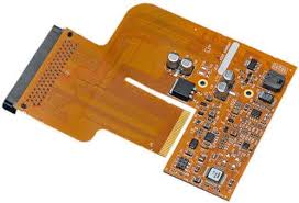
How are tolerances maintained in circuit board assembly?
Tight tolerances for critical components like plated hole diameters and traces can be achieved by using the right manufacturing processes, material specifications, and quality control measures. However, the cost and flexibility of alternative components and fabrication methods can sometimes allow PCB designers to use more relaxed tolerances for non-critical features, without compromising the performance or reliability of the final product.
Tolerances for plated and non-plated holes, as well as routed features, are specified on the PCB drawing. Maintaining these tolerances will ensure that the product assembles correctly, and is compatible with other components in the system.
For example, maintaining tolerances for copper width and spacing helps prevent signal distortion, overheating, and short circuits in demanding applications. The PCB fabricator can achieve these tolerances by using the right materials and manufacturing process, and implementing quality control measures such as statistical process control.
As a designer, it is important to clearly specify the desired tolerances for each PCB component and feature on the drawing. These tolerances will be compared to the actual measurements during inspection and verification, and any deviation from the required tolerances will be identified as a defective part. Often, this can be corrected by re-working the part, or by changing the design to avoid the problem in the future. This can reduce the time and cost of the manufacturing process, as well as improve the quality of the resulting product. The best way to minimize these defects is to use Design for Manufacturability guidelines, and to work closely with the PCB manufacturer throughout the manufacturing process.


