
printed circuit board power distribution
Minimizing voltage drops in printed circuit board (PCB) power distribution is crucial for ensuring stable and reliable operation of electronic devices. Voltage drops occur when there is resistance in the conductive paths through which power is delivered, leading to a reduction in voltage levels seen by components. Excessive voltage drops can result in degraded performance, malfunctioning of components, and even failure of the entire system. Therefore, several strategies are employed to minimize voltage drops and optimize power distribution throughout the PCB.
One of the primary techniques for minimizing voltage drops in printed circuit board power distribution is optimizing trace widths and conductor sizes. Larger trace widths offer lower resistance, allowing for higher current carrying capacity and reduced voltage drop. By selecting appropriate trace widths based on the expected current levels and considering factors such as copper weight and thickness, designers can ensure that power is distributed efficiently with minimal voltage loss along the traces.
Moreover, reducing trace lengths and optimizing routing configurations are essential for minimizing voltage drops in PCB power distribution. Longer traces result in higher resistance and increased voltage drop, particularly at higher currents. Therefore, designers strive to minimize trace lengths by carefully planning the layout and routing of power traces, ensuring that power is delivered as directly and efficiently as possible to components across the PCB. Techniques such as using shorter and more direct routing paths, minimizing the number of vias, and avoiding sharp turns or corners help to reduce resistance and voltage drop along the traces.
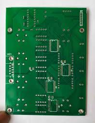
how do you minimize voltage drops in printed circuit board power distribution?
Additionally, optimizing the layer stackup and using multilayer PCBs can help minimize voltage drops in power distribution. Multilayer PCBs provide additional routing layers, allowing designers to create dedicated power and ground planes for efficient power delivery. By distributing power across multiple layers and minimizing the impedance between power and ground planes, designers can reduce voltage drop and ensure stable power distribution throughout the PCB. Proper layer stackup design, with consideration for power plane capacitance and impedance, further enhances power distribution efficiency and minimizes voltage drop.
Furthermore, selecting low-resistance materials and finishes for PCB fabrication can help minimize voltage drops in power distribution. Copper is commonly used as a conductor material in PCBs due to its low resistivity, which helps minimize voltage losses. Additionally, using high-quality copper with thicker plating or opting for gold or silver finishes on copper traces can further reduce resistance and voltage drop, particularly in high-current applications. By choosing materials and finishes with low resistivity, designers can optimize power distribution and ensure efficient delivery of power to components across the PCB.
Incorporating decoupling capacitors into the power distribution network is another effective strategy for minimizing voltage drops in PCBs. Decoupling capacitors act as local energy reservoirs, providing a stable supply of power to components and absorbing transient currents during sudden load changes. Placed strategically near power pins of integrated circuits and other high-current components, decoupling capacitors help to stabilize power supplies, reduce voltage ripple, and minimize voltage drops. Proper selection of capacitor values and placement locations is essential to effectively mitigate voltage drops and ensure reliable operation of electronic devices.
In conclusion, minimizing voltage drops in printed circuit board power distribution is essential for ensuring stable and reliable operation of electronic devices. By optimizing trace widths and conductor sizes, reducing trace lengths, optimizing layer stackup, selecting low-resistance materials and finishes, and incorporating decoupling capacitors, designers can effectively minimize voltage drops and optimize power distribution throughout the PCB. Through careful planning, design optimization, and adherence to best practices, designers can create power-efficient PCB designs that meet performance specifications and ensure the longevity and reliability of electronic devices.

